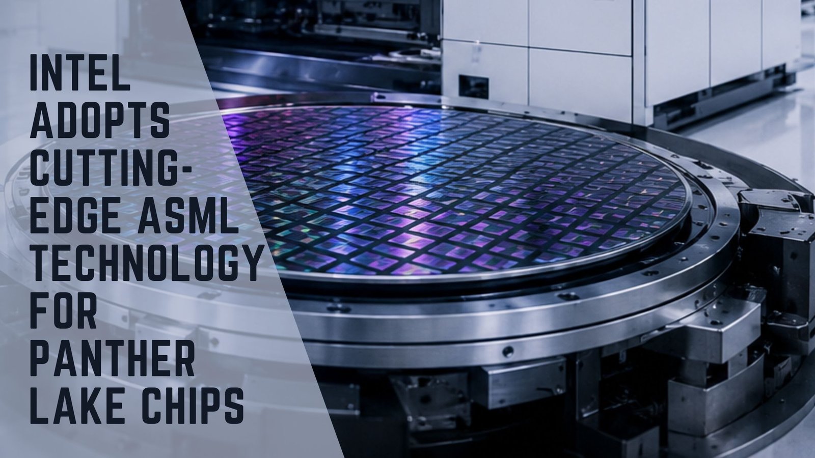
Intel’s Strategic Shift to Advanced Lithography Tools
Intel has taken a significant step in semiconductor manufacturing by integrating advanced machinery from ASML to produce its high-performance Panther Lake laptop chips. This strategic move, announced by ASML, is aimed at enhancing Intel’s ability to utilize these state-of-the-art tools effectively.
Embracing High NA EUV Technology
Starting with exploratory trials in 2024, Intel has embarked on utilizing ASML’s next-generation High Numerical Aperture (High NA) Extreme Ultraviolet (EUV) lithography machines. These sophisticated devices are pivotal in etching intricate circuit designs onto microchips, marking a new era in chip production for Intel’s Panther Lake processors.
Economic and Technical Considerations
The semiconductor industry has long debated the economic feasibility of deploying High NA tools, which are considered essential for future technological advancements. As chipmakers push the boundaries of miniaturization, these tools become increasingly important. However, the financial implications are substantial, with the High NA equipment priced at approximately $400 million—double the cost of standard EUV machines. The technical complexities involved in integrating these tools into existing manufacturing processes further compound the challenge.
Data Collection and Optimization
Intel plans to use the High NA tool selectively for specific chip layers, a strategic approach that facilitates data collection and equipment optimization. This not only enhances Intel’s manufacturing capabilities but also provides valuable insights for ASML to refine their technology.
Secrecy and Strategic Development
While Intel has refrained from commenting on this development, the move is indicative of its commitment to advancing its manufacturing prowess. The company employs its 18A process for crafting Panther Lake chips, with existing production already utilizing ASML’s standard EUV lithography machines. Lithography, a critical process in chip manufacturing, involves using light to create the complex patterns essential for circuit functionality.
Research and Development Initiatives
In 2024, Intel received its inaugural High NA tool at its research and development center in Hillsboro, Oregon. This facility serves as a hub for pioneering new manufacturing techniques and exploring cutting-edge technologies. The integration of High NA tools at this site underscores Intel’s dedication to maintaining a competitive edge in the semiconductor industry.
Implications for the Chipmaking Industry
The introduction of High NA EUV technology represents a transformative moment for Intel and the broader chipmaking sector. As the industry grapples with the ever-increasing demand for smaller, more powerful chips, the adoption of such advanced tools is likely to become a standard practice. This transition not only positions Intel as a leader in technological innovation but also sets the stage for future developments in semiconductor manufacturing.
Looking ahead, the successful deployment and optimization of High NA tools could redefine industry standards, paving the way for significant advancements in computing power and chip efficiency. Intel’s proactive approach in embracing these technologies reflects its strategic foresight and commitment to innovation.